usb
usb protocol engine
november 2024
pittsburgh, pa
18-341: logic design and verification
tools: systemverilog, vcs
Universal Serial Bus (USB) is the universal standard connecting keyboards, mice, flash drives, and chargers to computers. Connecting a flash drive requires a complex series of low-level electrical signals, handshakes, error checks, and data translations. This project designed the underlying silicon hardware engine (a Serial Interface Engine) that manages the electrical communication and protocols necessary to read data from external USB storage drives securely and reliably.
intro
A synthesizable USB 2.0 Host Serial Interface Engine (SIE) modeled in SystemVerilog and verified in simulation using VCS. Working entirely at the RTL level, the host implements a multi-threaded architecture that interfaces with an encrypted thumb drive model. The engine manages everything from physical-layer signaling and NRZI clock extraction to transaction-level error recovery and memory paging.
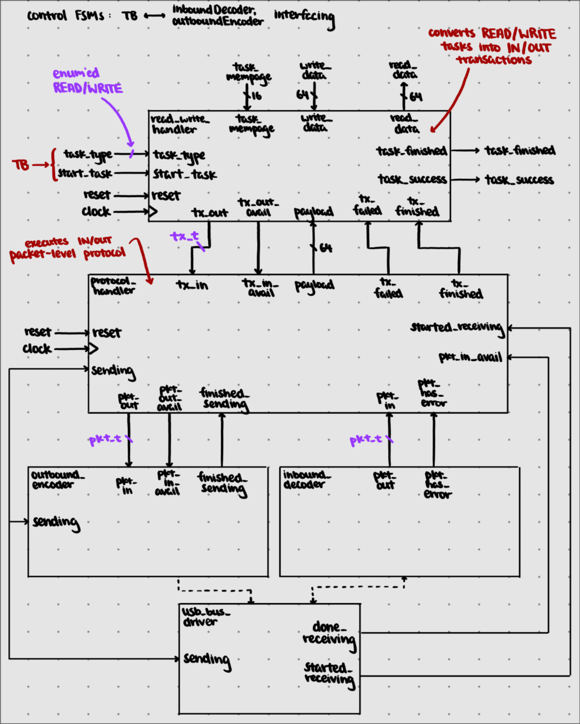
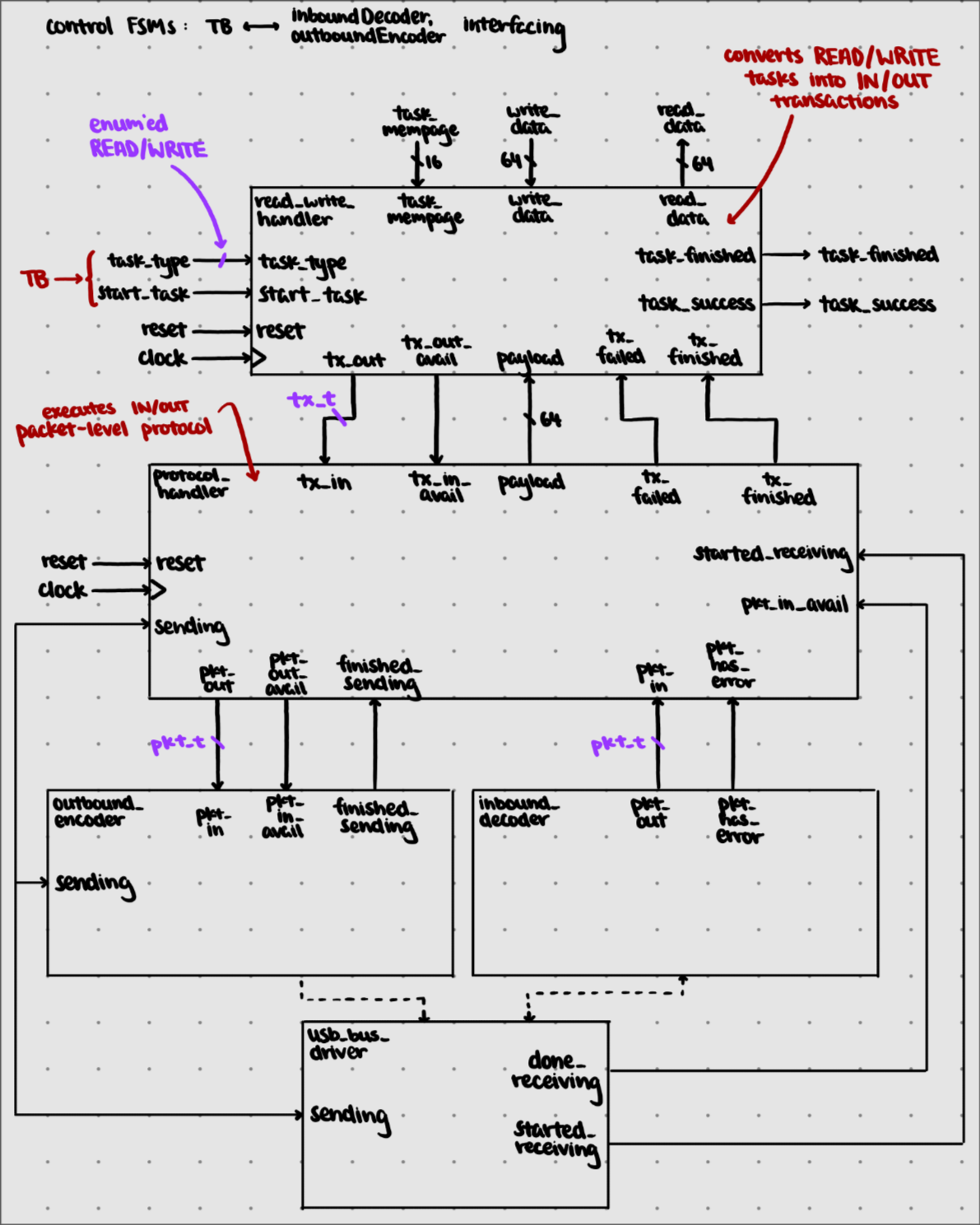
System block diagram of the USB Host.
bit-level engine
The lowest layer of the SIE translates the differential physical-bus signals (DP and DM) into clean data packets. Instead of storing large chunks of memory and executing software-style loops, we designed the transmit and receive pipelines as a series of low-latency hardware modules.
On the transmit path, the bitstream passes through:
- CRC Generators: Calculates 5-bit CRCs for token packets and 16-bit CRCs on the fly for data packets.
- Bit Stuffer: Monitored by a sequential tracker, it automatically inserts a zero-bit after detecting six consecutive ones to prevent receiver clock drift.
- NRZI Encoder: Toggles output states on zeros and maintains states on ones, using tri-state bus drivers to manage single-ended zero (SE0) sequences.
The receive path mirrors this flow, feeding raw bus states through an NRZI decoder, a bit unstuffer, and a parallel CRC checker.
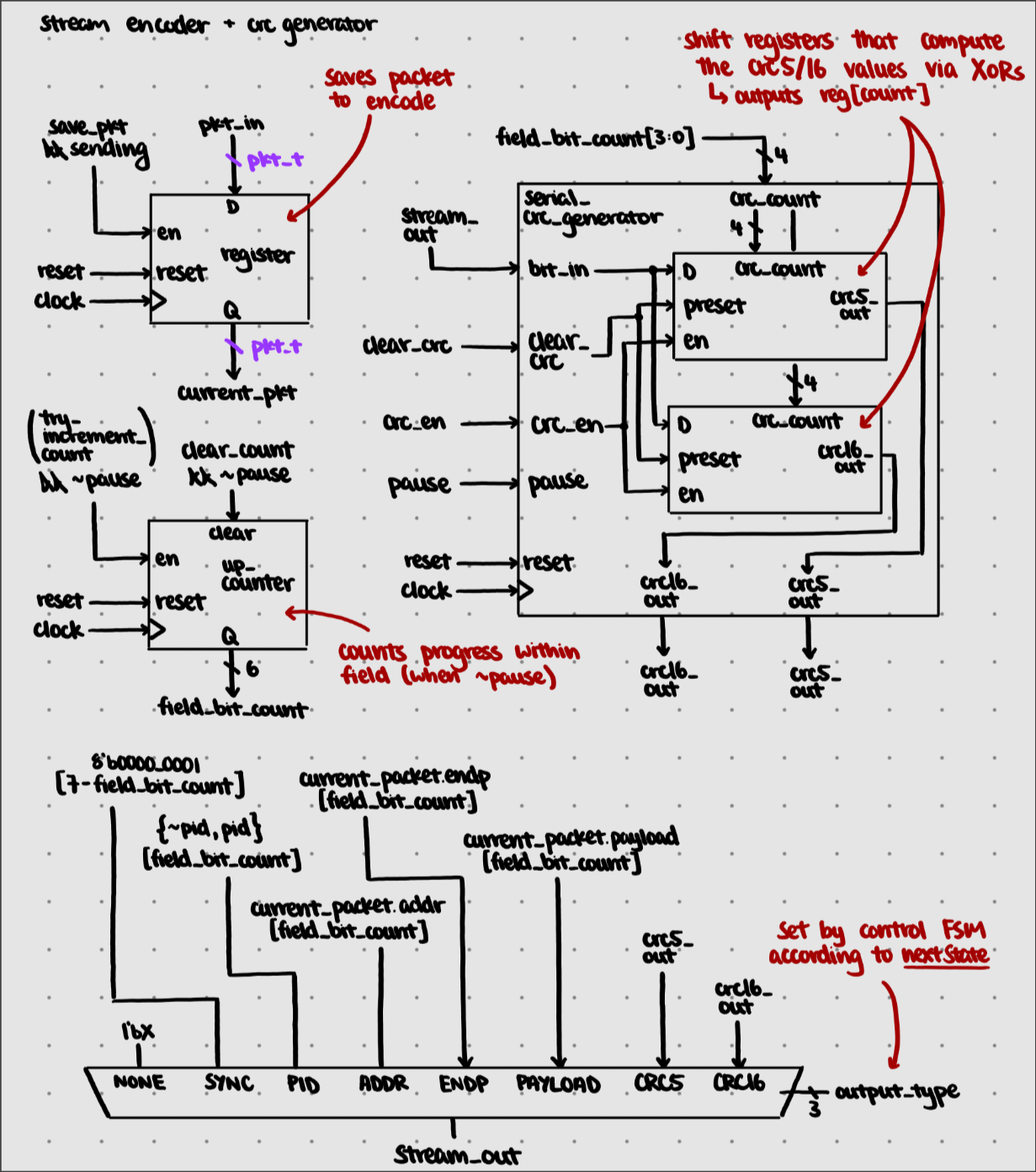
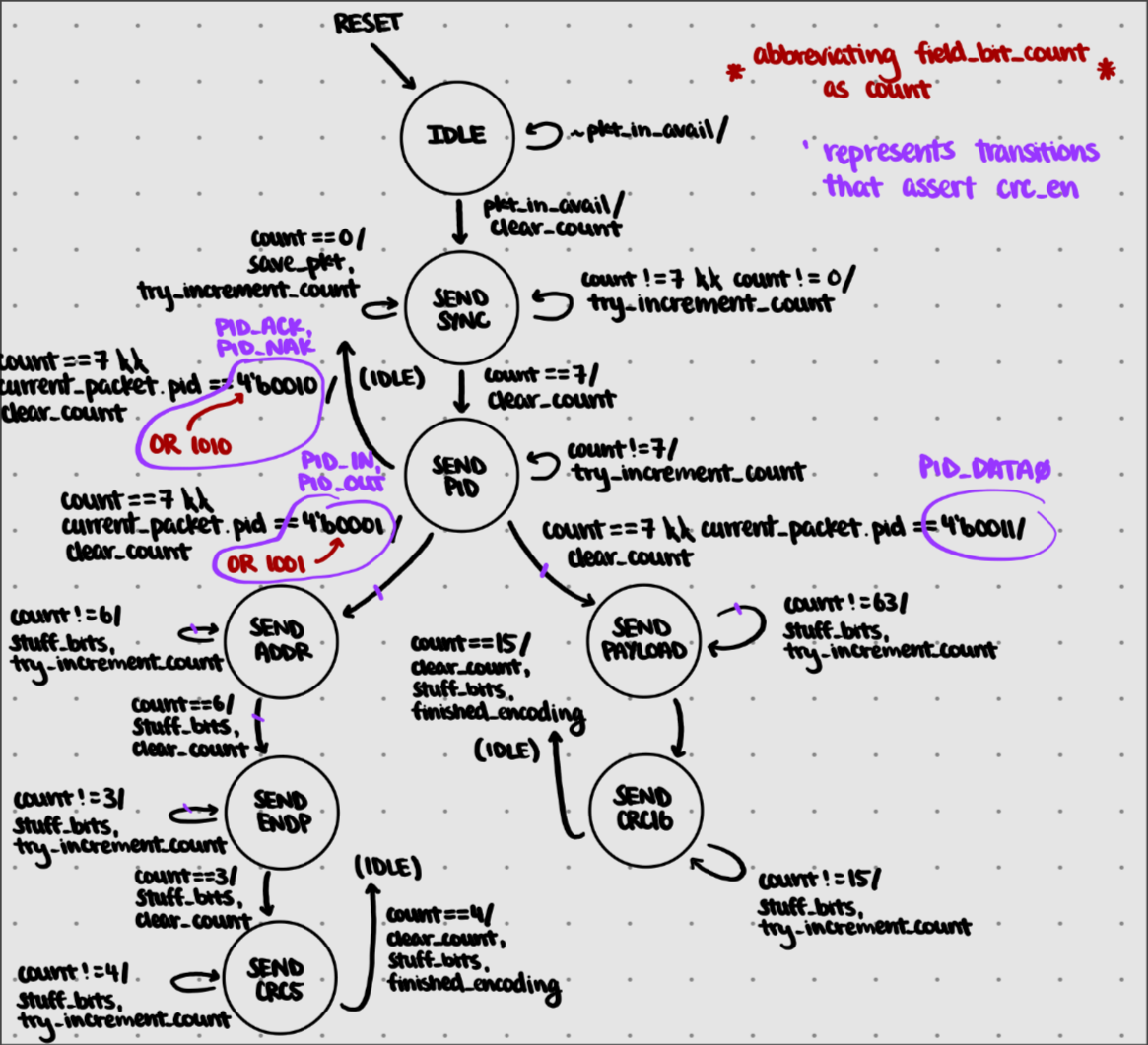
Stream encoder and CRC datapath/FSM layout.
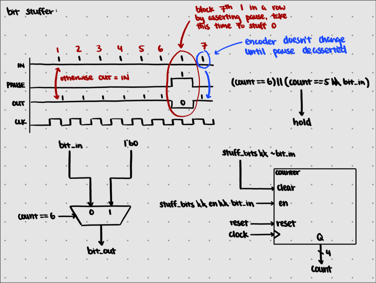
Bit stuffer module state machine and logic.
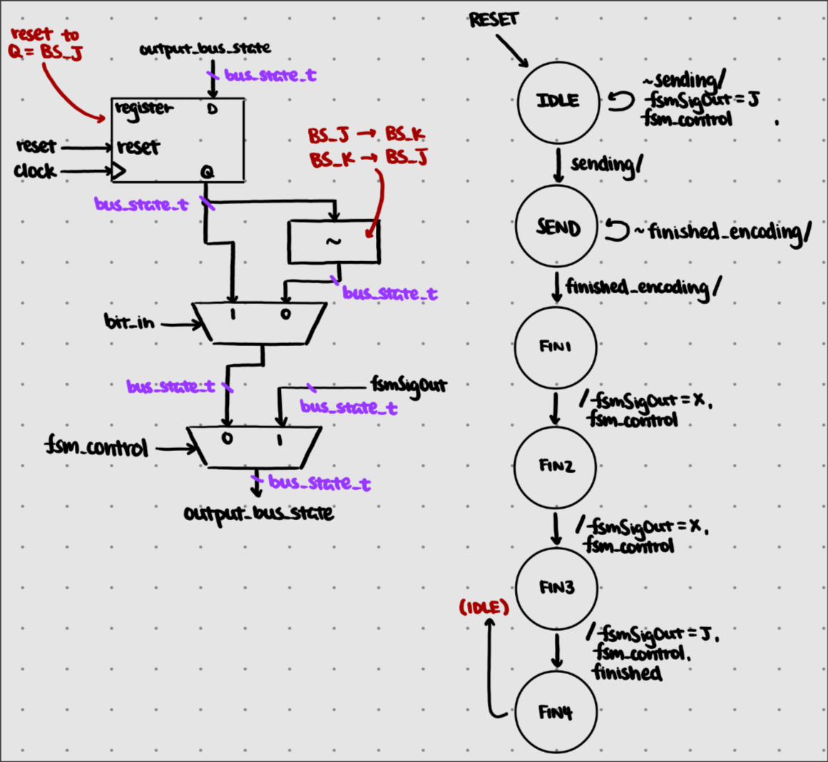
NRZI encoder/decoder datapath and FSM state transition diagrams.
protocol handler
Operating above the serial bitstream is the protocol and transaction management logic. The protocol handler receives high-level commands (like read or write requests to memory pages) and orchestrates them into standard USB packet sequences: OUT, IN, DATA0, ACK, and NAK.
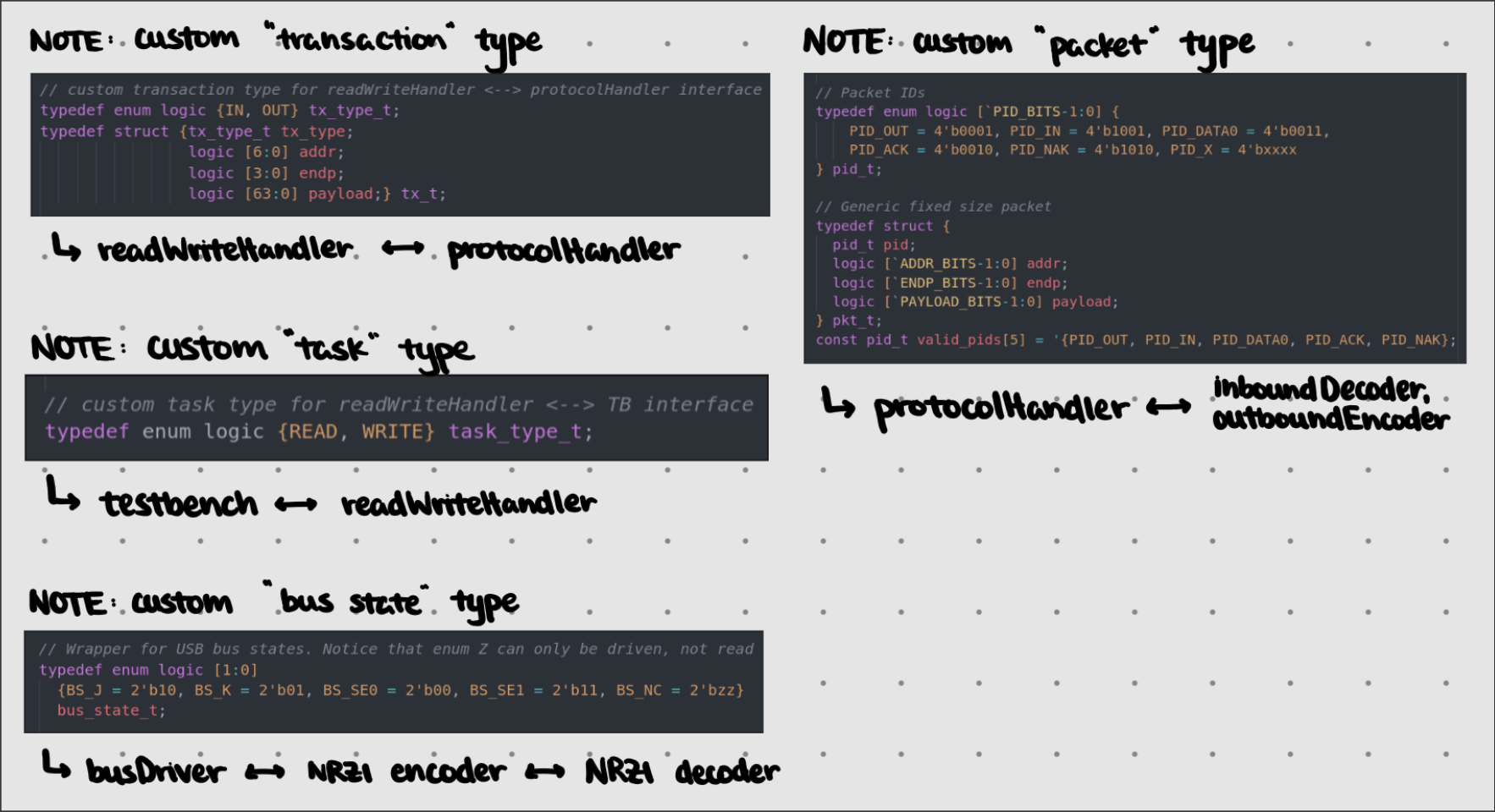
Custom SystemVerilog packet and transaction struct definitions.
Because real hardware is susceptible to noise and transmission errors, the protocol handler is governed by a robust error-recovery FSM.
- Timeout Detection: Uses an 8-bit timer to detect device silence, declaring a timeout if the device fails to respond within 255 clock cycles.
- NAK & Retry Arbitration: If a packet is corrupted (violating CRC residues) or times out, the host returns a NAK and retries the transaction.
- Failure Recovery: The FSM allows up to 7 retries per transaction before aborting the request, ensuring high transmission reliability.
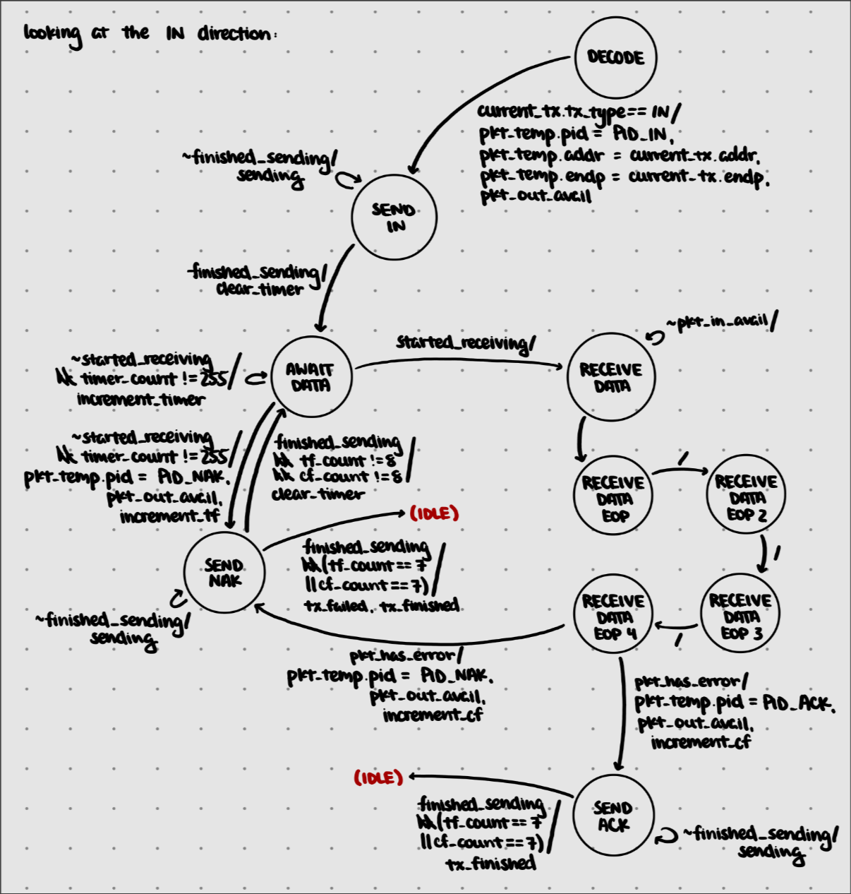
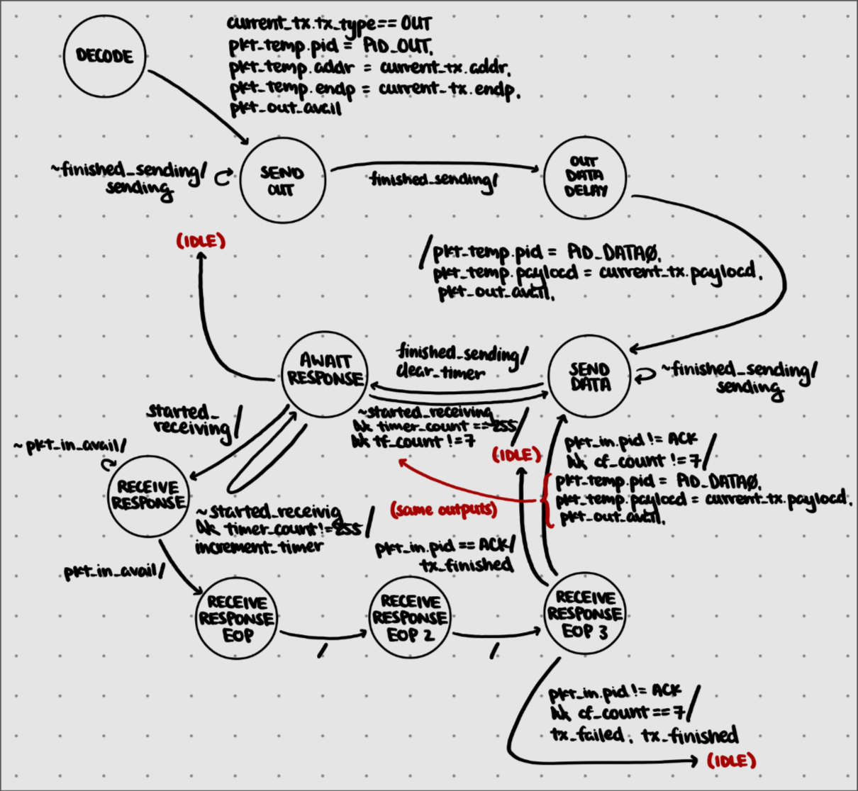
Protocol handler state machines for IN (left) and OUT (right) transactions.
verification & simulation
Since the design was validated entirely in simulation, we subjected our host to rigorous testbench suites designed to expose edge-case bugs. We ran simulated transfers under scenarios including:
- Edge Data Patterns: Inducing maximum bit-stuffing transitions and boundary-value CRC calculations.
- Stress Cycles: Executing 100 random sequential reads and writes to verify address paging logic and FSM stability.
- Fault Injection: Bombarding the bus with synthetic packet corruptions, timeouts, and abort scenarios to prove that the protocol handler successfully executes error recovery up to the 7-retry limit.
Thank you to the course staff in 18-341 for the simulation testbenches and checkoff support!