matmul
pipelined matrix multiplier
september 2024
pittsburgh, pa
18-341: logic design and verification
tools: systemverilog, vcs, quartus
Matrix multiplication is the fundamental mathematical operation behind Artificial Intelligence (like ChatGPT), graphics rendering, and computer vision. Calculating massive grids of numbers in software requires billions of sequential steps. This project built a dedicated silicon hardware engine (a pipelined systolic array) that solves giant matrix equations in parallel, dramatically speeding up AI calculations while using less energy.
intro
An optimized hardware-based matrix multiplier modeled in SystemVerilog, simulated and verified using VCS, synthesized with Altera Quartus Prime, and deployed onto a physical DE0-CV Development Board (Cyclone V FPGA). Operating entirely at the register-transfer level (RTL), the system computes the matrix equation $Y = A \times B + C$ directly on clock division and hardware pipelines, maximizing parallel throughput and satisfying a 70 MHz timing constraint.
matrix multiply
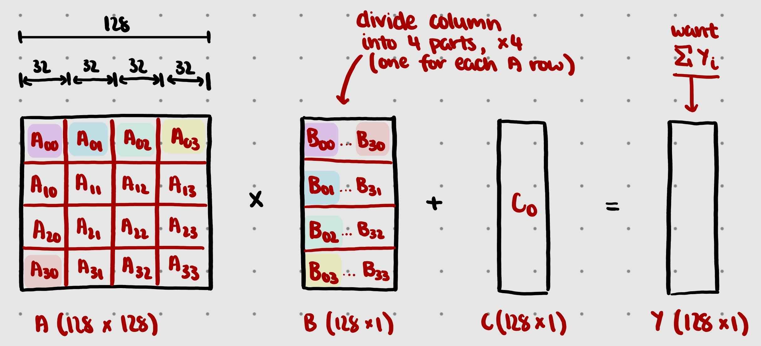
The core problem is to solve the matrix equation $Y = A \times B + C$, where $A$ is a $128 \times 128$ matrix (8-bit values), $B$ is a $128 \times 1$ column vector (8-bit values), and $C$ is a $128 \times 1$ column vector (16-bit values). The final objective is to output the sum of all elements in the resulting 24-bit $Y$ vector.
Rather than computing the vector $Y$ element-by-element and storing intermediate vectors (which would require excessive memory and clock cycles), we algebraically simplified the summation: $$Result = \sum_{i=0}^{127} Y_i = \sum_{i=0}^{127} \left( \sum_{j=0}^{127} A_{ij} B_j + C_i \right)$$
This mathematical reformulation allowed us to separate the design into two parallel processing pathways: one that accumulates the matrix product $A \times B$ and another that sums the elements of vector $C$ independently.
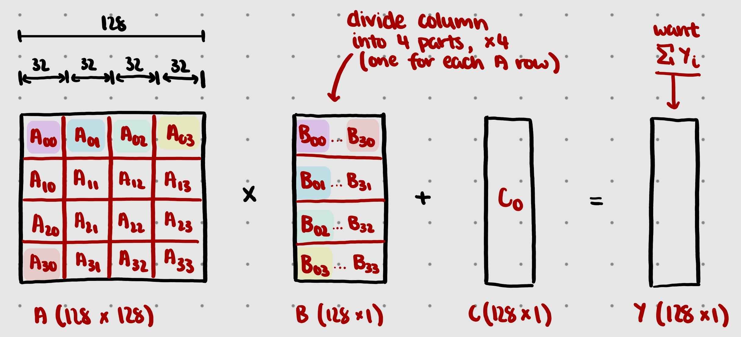
RAM/ROM layout mapping out how matrices A, B, and C are stored on the Cyclone V's block RAMs.
parallel architecture & pipelining
To achieve high clock-cycle efficiency, we designed a highly parallelized pipeline that utilizes 272 of the board’s 308 available M10K block RAMs and 32 of its 198 embedded multipliers.
Our architecture instantiates 16 parallel MiniMultiplier modules. Leveraging the dual-port capabilities of the M10K RAMs, each module reads two adjacent values (horizontally in $A$ and vertically in $B$) simultaneously per clock cycle using both memory ports. Two combinational multipliers ($A_1 \times B_1$ and $A_2 \times B_2$) calculate the products, which are added together via a register.
Parallel execution pathway for multiplying A and B, showing 16 mini-multiplier lanes.
To aggregate the output of these 16 parallel lanes without creating a massive combinational path that would violate our 70 MHz clock limit, we built a 4-tier pipelined reduction tree. Each tier uses custom AdderRegister modules to sum pairs of intermediate values and latch the results. The final tier adds the sum to a running total register over cycles 9 to 520, completing the $A \times B$ accumulation in exactly 521 cycles.
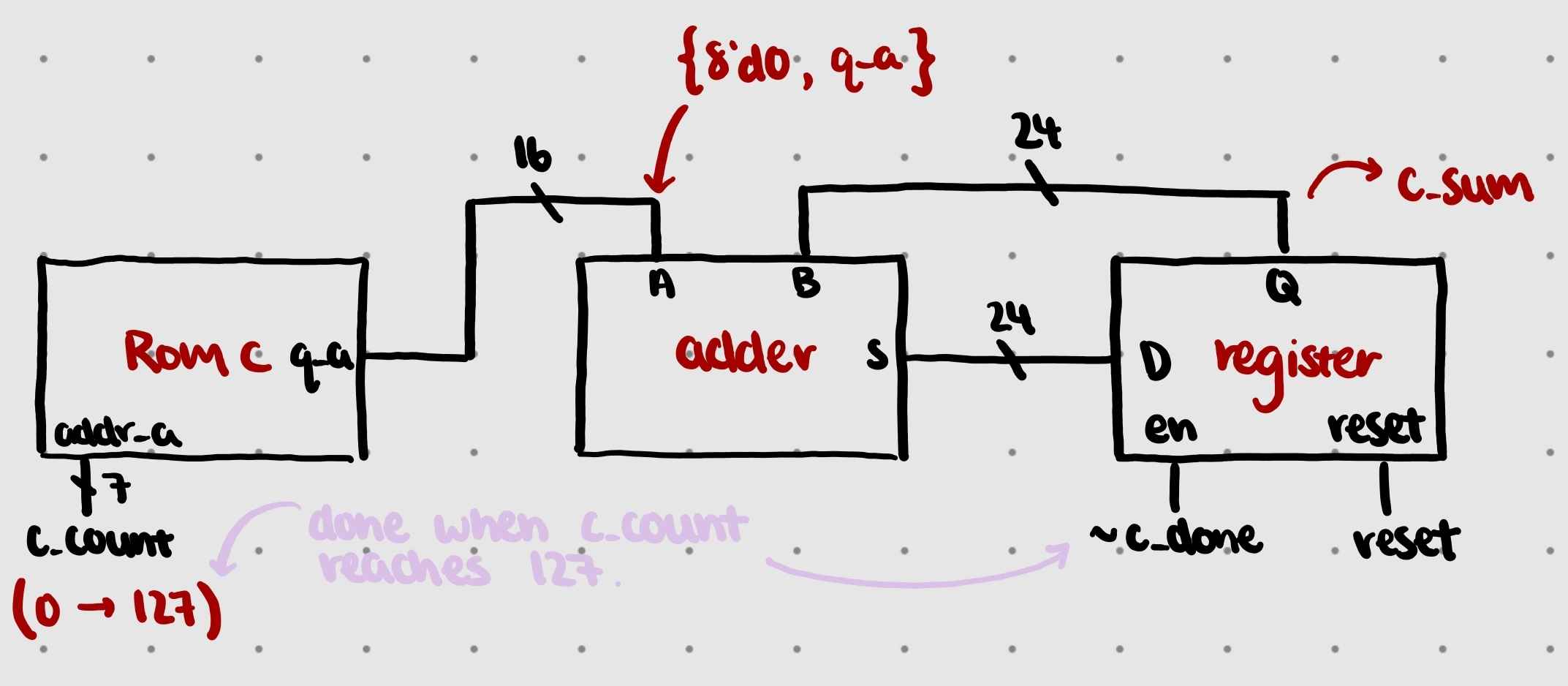
Sequential accumulator pathway used to sum vector C elements.
For vector $C$, we read its 128 elements sequentially, accumulating their sum directly in a register. Because this pathway only requires 128 cycles, it completes long before the $A \times B$ pathway. The final sum of $Y$ is produced by adding the accumulated products and vector $C$’s sum together.
controls & debugging
For user interaction, we configured SW[0] on the DE0-CV board to toggle the 7-segment hex display output (HEX5 to HEX0). Setting the switch to 1'b0 displays the final 24-bit accumulated sum, while setting it to 1'b1 displays the total clock cycle count required to run the computation.
Additionally, we routed internal execution signals (such as done, active, and count flags) directly to the board’s LEDs (LEDR), providing a real-time hardware status monitor for diagnostic testing.
Thank you to the course staff in 18-341 for the lab resources and compilation support!