
hydra
28nm digital ic tapeout
january 2026 - present
pittsburgh, pa
18-725: advanced digital ic design
teammates: sophia fu, kody liang, silvia song, kaylan zhang
mentors: ken mai, larry tang, siddharth das
tools: chisel, spinalhdl, systemverilog, vexriscv, cocotb, genus, innovus, calibre, xcelium
Transmitting encrypted data securely over the internet and processing high-speed signals (like 5G, audio, or video) require immense mathematical calculations. Encryption uses Number Theoretic Transforms (NTT) to protect data against future quantum computers, while signal processing uses Fast Fourier Transforms (FFT) to process waves. HYDRA is a physical silicon chip (a 28nm System-on-Chip) that combines both algorithms into a single shared hardware engine, giving electronic devices high-speed signal processing and next-generation quantum-safe security on a single tiny chip.
overview & high-level architecture
HYDRA (Hybrid Dual Reconfigurable Architecture) is a custom System-on-Chip (SoC) designed and taped out in a 28nm digital IC technology node. The chip is designed to accelerate two mathematically similar but traditionally disparate workloads: Fast Fourier Transforms (FFTs) for digital signal processing, and Number Theoretic Transforms (NTTs) for post-quantum lattice-based cryptography (specifically targeting Kyber/ML-KEM algorithms).
Both FFT and NTT algorithms rely on a butterfly network topology to execute Cooley-Tukey decimation-in-time/frequency passes. By sharing the butterfly routing infrastructure and multiplexing the complex-floating-point and modular-integer arithmetic units, HYDRA provides a hardware accelerator that is highly area-efficient while serving dual-mode operations.
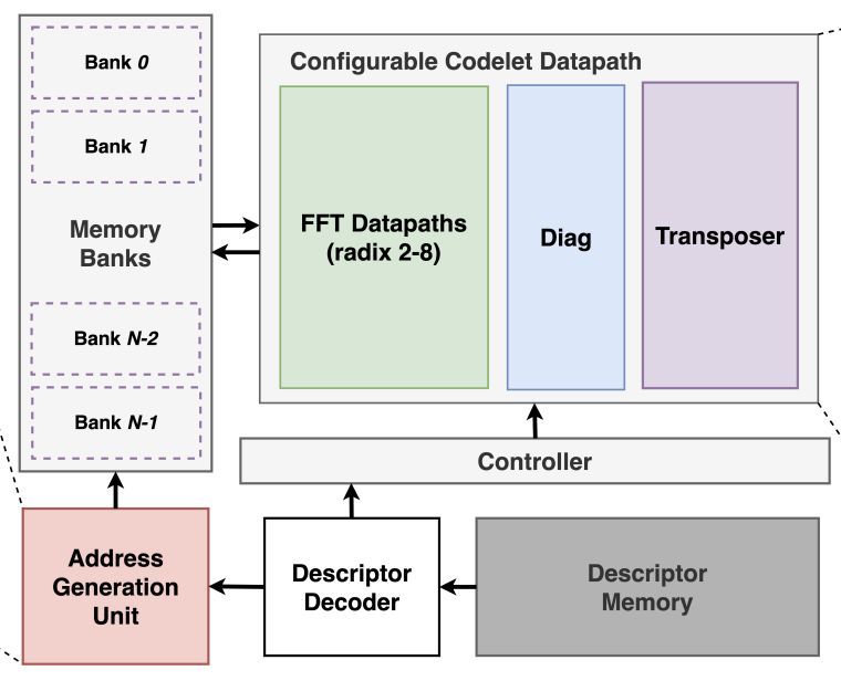
Figure 1: HYDRA Accelerator Architecture (L. Tang et. al, 2025).
reconfigurable accelerator design
At the core of the HYDRA accelerator lies a reconfigurable butterfly unit that dynamically switches between two dataflows:
- FFT Mode: Configured for 8-point radix-2 Cooley-Tukey FFT operations using standard IEEE-754 complex floating-point numbers. The arithmetic units operate on complex data inputs (real and imaginary parts), utilizing complex adders and complex multipliers.
- NTT Mode: Configured for modular integer arithmetic in lattice ciphers. In this mode, the complex adder/subtractor and multiplier structures are dynamically remapped into modular arithmetic units (modulo addition, modulo subtraction, and modulo multiplication). The hardware features a dedicated Barrett Reduction engine to perform high-speed modulo calculations on the fly without costly division operations.
The butterfly network is governed by a fully pipelined accelerator controller designed in Chisel (Scala). It generates addresses dynamically via specialized Address Generation Units (AGUs) that handle multi-dimensional strides, batch offsets, twiddle factor lookups, and block transposes directly out of local memory banks.
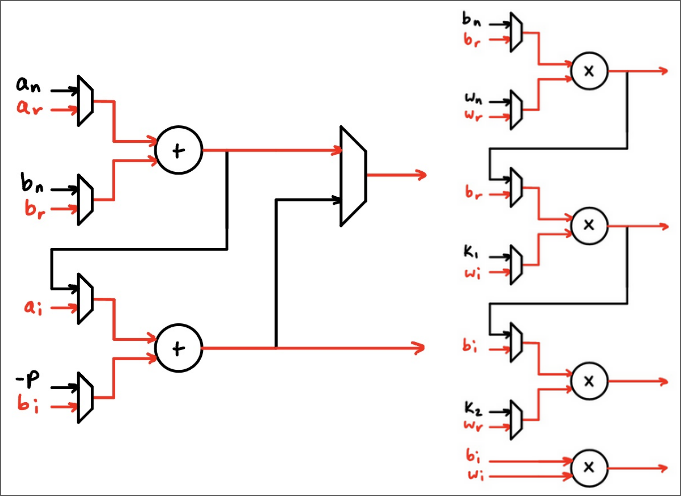
Figure 2: Reconfigurable modular arithmetic units set up for FFT mode.
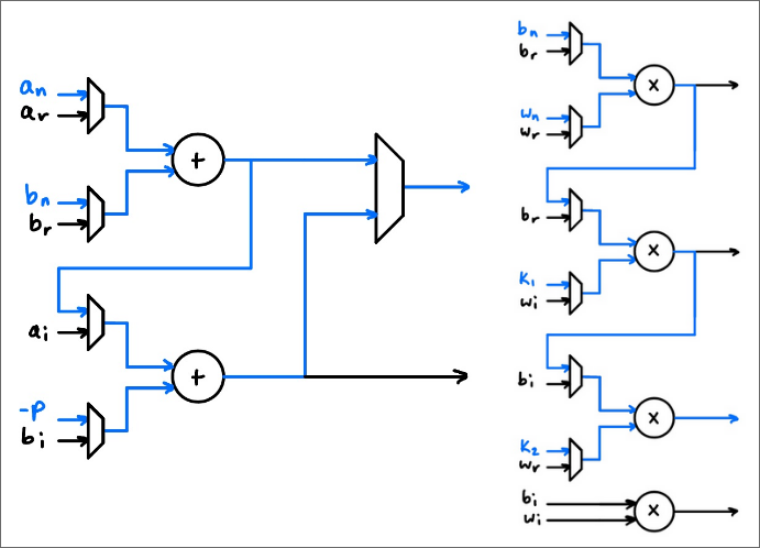
Figure 3: Reconfigurable modular arithmetic units set up for NTT mode.
system-on-chip (soc) integration
To provide full system programmability, the HYDRA accelerator is integrated into a complete System-on-Chip (SoC) centered around a 32-bit VexRiscv CPU core.
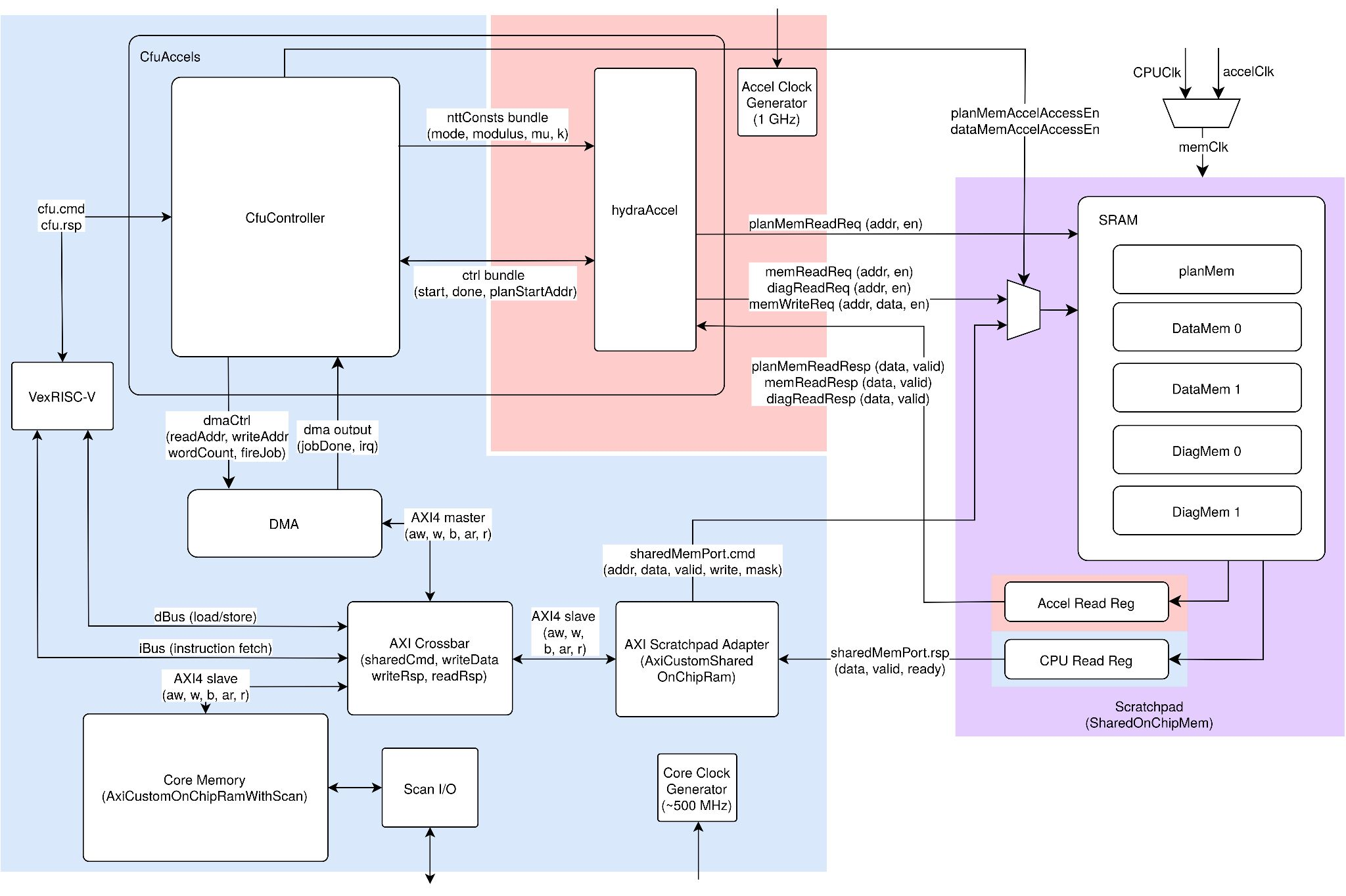
Figure 4: HYDRA Full System Architecture & Memory Map.
Key features of the SoC integration include:
- CFU (Custom Function Unit) Interface: Tightly couples the CPU and accelerator, enabling low-latency control handshakes. Start, configuration constants (e.g., modulus value, modular inverse parameters), and done status signals are handled instantly through custom instruction extensions.
- Shared “Scratchpad” Memory: A banked, dual-port local SRAM ($32\ \text{kB}$ data memory, $1\ \text{kB}$ instruction/plan memory) shared between the VexRiscv CPU and the accelerator. A hardware multiplexer coordinates control: while the CPU writes inputs or reads outputs, the accelerator is locked out, and vice-versa. This eliminates read-write hazards and avoids the overhead of bus-arbitration protocols.
- DMA Engine: The CPU configures a high-performance DMA controller to move contiguous blocks of data between main system memory and the shared scratchpad memory, ensuring the accelerator is continuously fed with minimal CPU intervention.
- C Software API: A custom low-level C firmware library using the plan/execute paradigm (interfacing with the FFTX backend). Users compile standard C programs targeting the accelerator, wrapping custom assembly instructions into clean function calls.
verification & simulation suite
Verification was performed using a custom testbench suite powered by cocotb (python-based HDL verification) and Cadence XCelium.
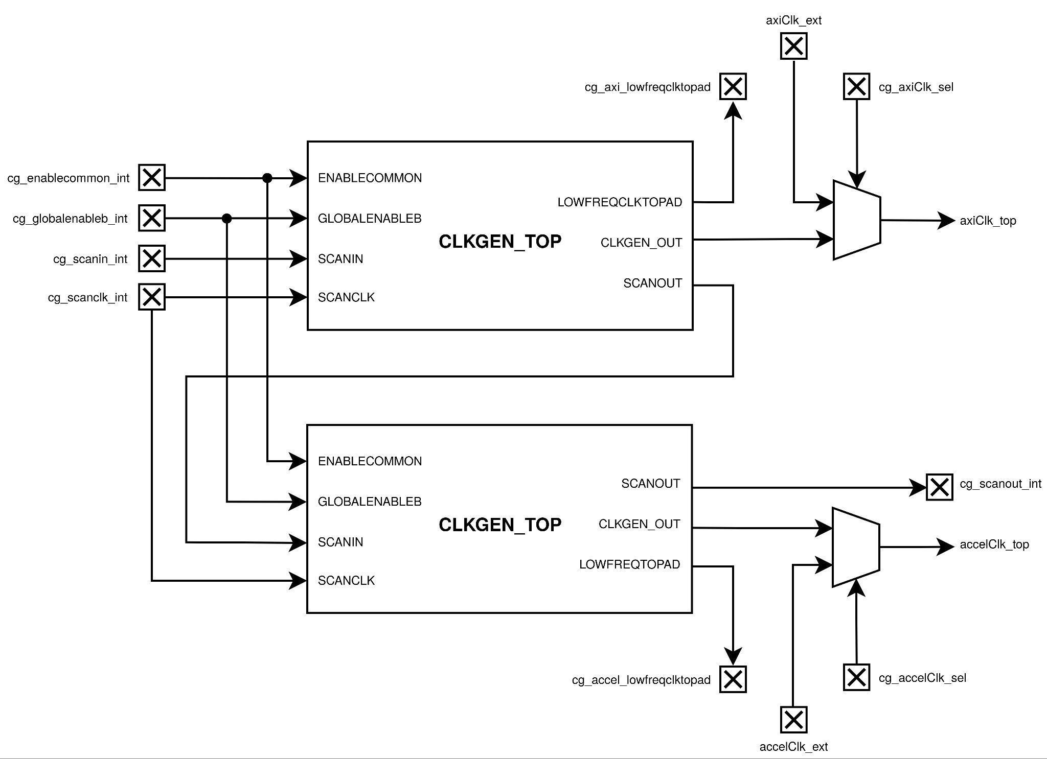
Figure 5: SoC Clock Generation & Scan Configuration.
Our verification strategy guaranteed correctness at every design phase:
- Equivalence Across Netlists: Simulating and matching test vectors across RTL, post-synthesis gate-level netlists, and final post-signoff netlists.
- Infrastructure Checks: 10/10 functional test suites verifying stand-alone radix-2 butterfly operations, CFU configurations, DMA data transfers, shared memory accessibility, and CPU print buffers.
- DFT & Silicon Testability: Integrated sequential Design-for-Test (DFT) scan chains. Verification runs simulated scanning programs directly into the VexRiscv memory to guarantee the scan chains would operate correctly on physical silicon post-fabrication.
physical design & tapeout
The chip layout was synthesized using Cadence Genus and placed and routed using Cadence Innovus in a 28nm process technology. Physical sign-off (DRC, LVS, and antenna checks) was achieved using Siemens Calibre.
| Metric | Target Value | Actual Result |
|---|---|---|
| Technology Node | 28nm | 28nm |
| Operating Frequency | $750\ \text{MHz}$ | $1.0\ \text{GHz}$ |
| Core Voltage | $0.9\ \text{V}$ | $0.9\ \text{V}$ |
| Power Consumption | $130.0\ \text{mW}$ | $135.2\ \text{mW}$ |
| Active Area | $0.5\ \text{mm} \times 0.5\ \text{mm}$ | $0.5\ \text{mm} \times 0.5\ \text{mm}$ |
| Area Utilization | - | $41.3\%$ |
| DRC / LVS Sign-off | Pass | Pass |
power & floorplanning
To optimize routing and limit IR drop, the layout was designed with three isolated power domains (Pad Ring, Clock Generators, and SoC Core) using power grids distributed on M4/M5 and M8/M9 metal layers.
The floorplan splits the memory macros to optimize access paths: CPU memory banks are placed in the top half, while the accelerator memories (data and twiddle factor banks) occupy the bottom half. By placing the data banks opposite each other, we facilitated low-latency ping-pong access patterns for Cooley-Tukey stages.
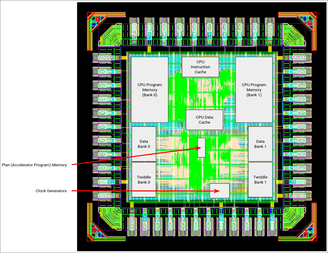
Figure 6: Final Chip Floorplan.
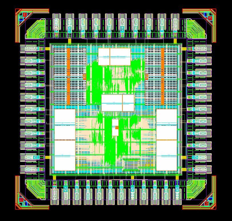
Figure 7: Final Tapeout GDS Layout.
area breakdown
| Unit | Subunit | Cell Count | Area ($\mu\text{m}^2$) | Area (%) |
|---|---|---|---|---|
| Vex CPU | Core | $9,168$ | $55,083.859$ | $13.33\%$ |
| Program Memory | - | $112,828.229$ | $27.31\%$ | |
| DMA Engine | $6,296$ | $16,927.982$ | $4.10\%$ | |
| Hydra Accel | Codelet Datapath | $31,161$ | $61,065.252$ | $14.78\%$ |
| Controller | $2,007$ | $5,154.163$ | $1.25\%$ | |
| Other | $1,066$ | $2,675.452$ | $0.65\%$ | |
| Shared Mem | Program Memory | - | $3,418.787$ | $0.83\%$ |
| Data Memory | - | $77,922.016$ | $18.86\%$ | |
| Other | Routing, clock, power | $4,257$ | $78,002.178$ | $18.88\%$ |
| Total | - | $54,347$ | $413,077.918$ | $100.00\%$ |