sram
memory design and layout
november 2025
pittsburgh, pa
18-622: digital ic design
teammates: kody liang
tools: virtuoso
Static Random-Access Memory (SRAM) is the ultra-fast memory built directly inside computer processors (L1/L2 caches) to hold data for immediate calculation. Because SRAM cells operate at gigahertz speeds, they determine how quickly a chip can access data. This project designed a 4,096-cell SRAM memory chip at the individual transistor level on a 45-nanometer silicon process, optimizing layout geometry so memory reads and writes execute in under a nanosecond.
intro
A custom-designed, transistor-level 256 words × 16 bits SRAM (4,096 memory cells total) designed and laid out in Cadence Virtuoso using the GPDK045 (45nm) process technology. We optimized the memory architecture for speed, power, and layout density, achieving a clock frequency of 1.096 GHz in the worst-case TTLH process corner while maintaining a cell area efficiency of 58.26%.
architecture & floorplan
The memory array is partitioned into a pseudo-inverted-T floorplan to balance wordline and bitline delays:
- Subarray Partitioning: The 4,096 cells are split into two symmetric 64 × 32 cell subarrays.
- Central Row Decoders: Row decoders are placed in a single central column between the two subarrays. Driving the wordlines (WL) from the center halves the wire resistance to the far edges of the array, reducing wordline propagation delay.
- Column Multiplexing: We implemented a 4:1 column multiplexing factor. Each group of 4 columns shares a single bitline reset block at the top and a cell I/O block at the bottom.
- I/O Pitch Matching: The read column muxes, write column muxes, StrongArm sense amplifiers, and write drivers are co-designed to fit within the vertical pitch of 4 cell columns, eliminating routing congestion.
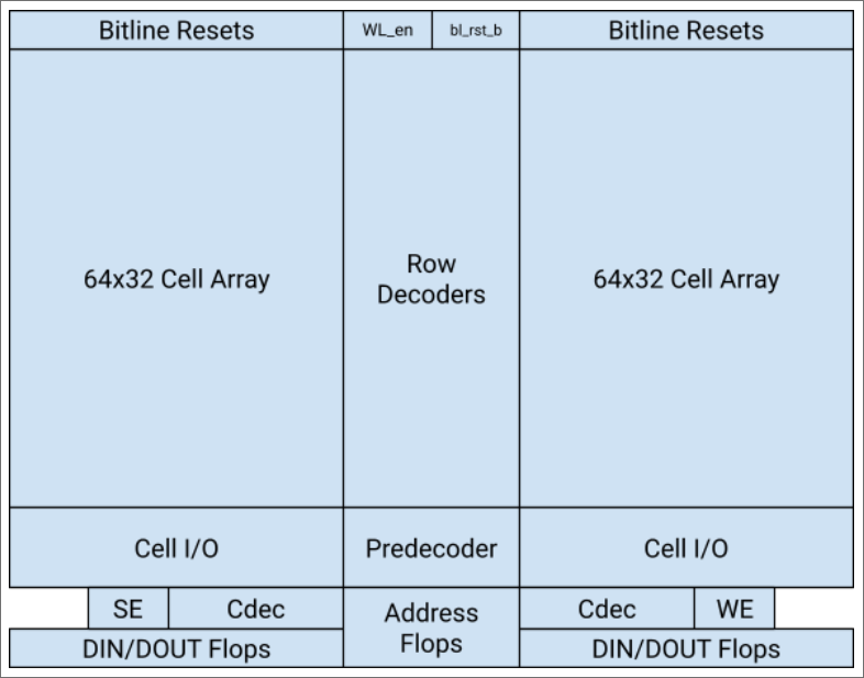
Pseudo-inverted-T floorplan diagram spanning two symmetric 64x32 cell arrays with central row decoders.
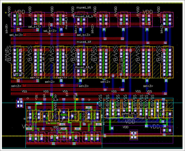
Layout of Cell I/O block, containing read/write multiplexers, StrongArm sense amplifier, and write driver.
circuit design & cell optimization
To ensure robust operation across process, voltage, and temperature (PVT) variations, every component was sized through rigorous analysis:
- 6T SRAM Cell: The core storage element is a standard 6-transistor (6T) cell. Transistors were sized to balance read stability and writeability, achieving a Read Static Noise Margin (Read SNM) of 498.8 mV and a maximum read current of 563.7 nA.
- StrongArm Sense Amplifier: We utilized a StrongArm Sense-Amplifier Flip-Flop (SAFF) at the bottom of the read multiplexer. The latch-based structure resolves small bitline differentials quickly with zero static power dissipation.
-
Control Signal Generation: To save power, we bypassed the overhead of replica bitlines. Instead, we designed local inverter delay chains to generate the control pulses (Wordline Enable
WL_en, Sense EnableSE, Write EnableWE, and Bitline Resetbl_rst_b) relative to the clock.
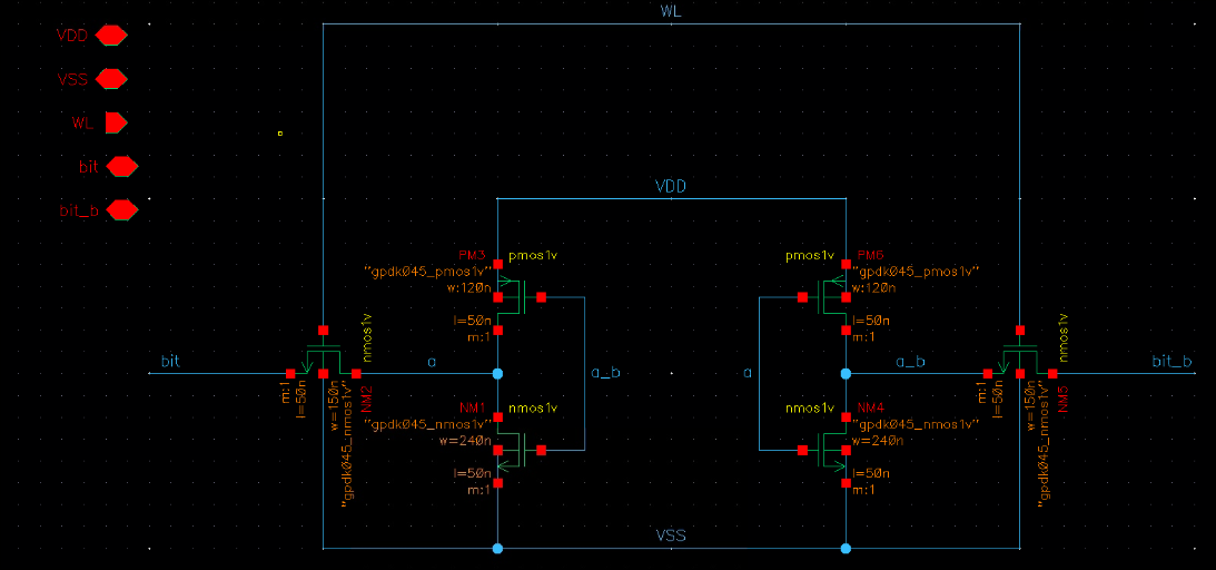
Transistor-level schematic of the 6T SRAM cell (two cross-coupled inverters with access transistors).
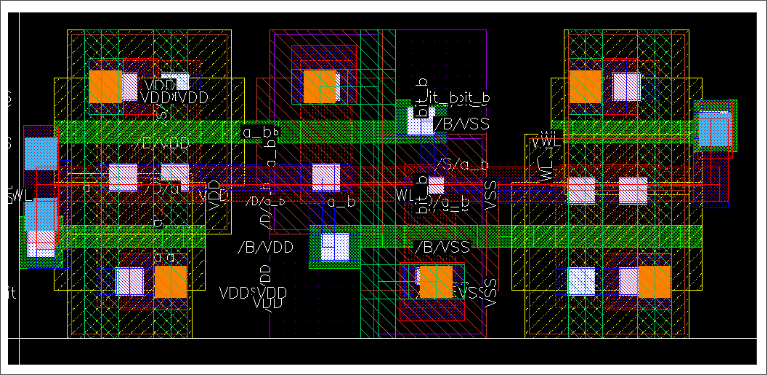
Physical symmetric layout of the 6T cell in Cadence Virtuoso (GPDK045 process).
verification & layout results
Interconnect resistance and capacitance for long global wires (e.g. clock, wordlines on Metal 6/2, and bitlines on Metal 3) were modeled with RC $\pi$-networks and verified using post-layout parasitic extraction (Assura AV_extract).
- Performance: Achieved a 912 ps cycle time (1.096 GHz) under the worst-case TTLH process corner.
- Power: Consumes 2.053 mW of total power at a 50/50 read/write mix (1.662 mW dynamic, 391 $\mu$W static).
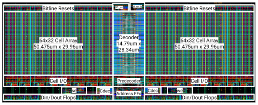
- Area: The complete layout fits in a compact bounding box of $115.7 \mu m \times 44.865 \mu m$ ($5,191 \mu m^2$), yielding an overall cell area efficiency of 58.26%.
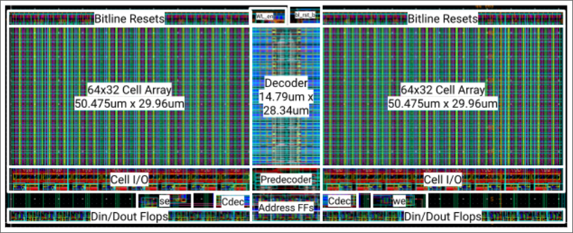
Complete silicon layout bounding box (115.7μm x 44.865μm) showing the pseudo-inverted-T symmetry.
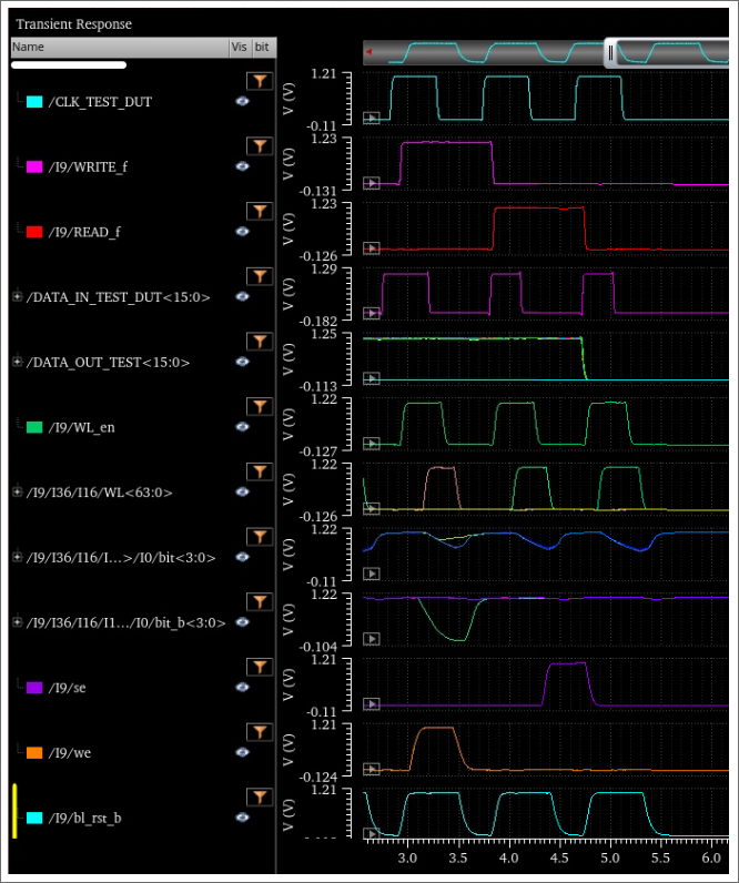
Analog simulation waveforms exercising the critical path read operation under worst-case timing.